Document Reference : International Rectifier AN-1162 Compensator design procedure for buck converter with voltage mode error amplifier Introduction to synchronous buck converter: Low ESR and Low ESL MLCC capacitors are used : High resonance frequency hence it will have ripple of high switching frequencies at low voltages levels. This is a desirable trait. But stabilizing a MLCC based compensator is more complex than compensator design using an Electrolytic capacitor - Need more attention.
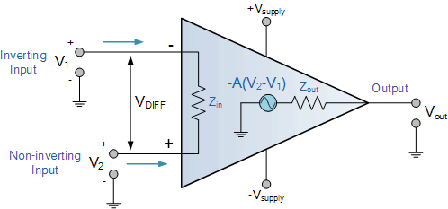
Opamps Operational amplifiers are linear devices that have all the properties required for nearly ideal DC amplification and are therefore used extensively in signal conditioning, filtering or to perform mathematical operations such as add, subtract, integration and differentiation. An Operational Amplifier , or op-amp for short, is fundamentally a voltage amplifying device designed to be used with external feedback components such as resistors and capacitors between its output and input terminals. These feedback components determine the resulting function or “operation” of the amplifier and by virtue of the different feedback configurations whether resistive, capacitive or both, the amplifier can perform a variety of different operations, giving rise to its name of “Operational Amplifier”. Transistor Y our brain contains around 100 billion cells called neurons—the tiny switches that let you think and remember things. Computers contain billions ...
Comments
Post a Comment